Introduction
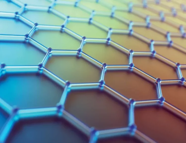
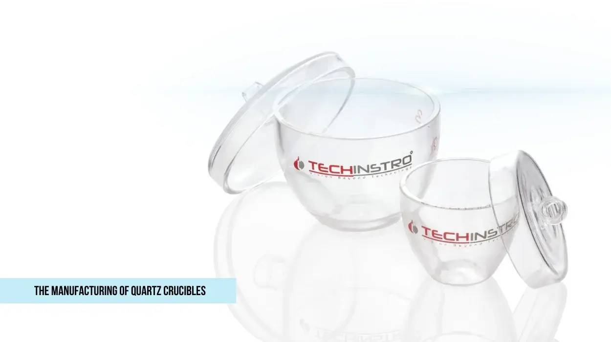
Quartz crucibles are essential in semiconductor manufacturing and are used to grow ultra-pure silicon crystals for computer chips. These crucibles must withstand extreme temperatures (over 1,700°C) while preventing contamination. But how are they made? This article explores the step-by-step manufacturing process, key challenges, and innovations shaping the industry.
Raw Material Selection: The Quest for Ultra-Pure Quartz
The process begins with selecting the right quartz material:
- Natural vs. Synthetic Quartz
- TypePuritySourceUse Case
- Natural Quartz 99.9%+ Mined crystals Lower-cost applications
- Synthetic Quartz (Fused Silica) 99.9999% (6N) Silicon tetrachloride (SiCl₄) gas Semiconductor-grade crucibles
- Synthetic quartz is preferred for high-end crucibles due to fewer impurities (Fe, Al, Na).
- Natural quartz is cheaper but requires extensive purification.
Step-by-Step Manufacturing Quartz Crucibles Process
Step 1: Melting & Homogenization
- Crushed quartz is melted in an electric arc furnace (3,000°C+) to remove bubbles and impurities.
- The molten quartz is stirred to ensure uniformity.
Step 2: Molding the Crucible
- The molten quartz is poured into a graphite mold shaped like a crucible.
- Rotational molding ensures even thickness and prevents defects.
Step 3: Annealing (Slow Cooling)
- The crucible is cooled in a controlled kiln to prevent stress cracks.
- Too-fast cooling causes microfractures, making the crucible unusable.
Step 4: Precision Machining & Polishing
- The crucible is CNC-machined to exact dimensions (for Czochralski crystal growth).
- The inner surface is mirror-polished to minimize silicon sticking.
Step 5: Coating (Optional but Critical for High-End Crucibles)
- A thin layer of yttria (Y₂O₃) or silicon nitride (Si₃N₄) is applied to:
- Reduce devitrification (crystallization at high temps).
- Prevent oxygen leakage into the molten silicon.
Step 6: Quality Control & Testing
- Bubble inspection (X-ray/ultrasound scanning).
- Purity check (mass spectrometry for trace metals).
- Thermal shock test (rapid heating/cooling cycles).
Innovations in Quartz Crucible Production
- AI & Machine Learning for Defect Detection
- Computer vision scans crucibles for microcracks before they fail.
- Predictive analytics forecasts crucible lifespan in production.
- Larger Crucibles for 450mm Wafers
- The shift to bigger wafers demands larger, more stable crucibles.
- Challenges: Thermal stress increases, requiring stronger materials.
- Sustainable Manufacturing
- Recycled quartz crucibles (after reconditioning) reduce costs by 20-30%.
- Low-energy plasma melting cuts carbon footprint.
The Future: What’s Next for Quartz Crucibles?
Self-healing coatings that repair minor cracks during use.
Hybrid crucibles (quartz + advanced ceramics for longer life).
Quantum computing demands may require even purer materials.
Conclusion
Quartz crucible manufacturing is a high-precision science that balances material purity, thermal stability, and mechanical strength. As semiconductor technology advances, crucibles must evolve, too—whether through AI-driven quality control, new coatings, or sustainable production