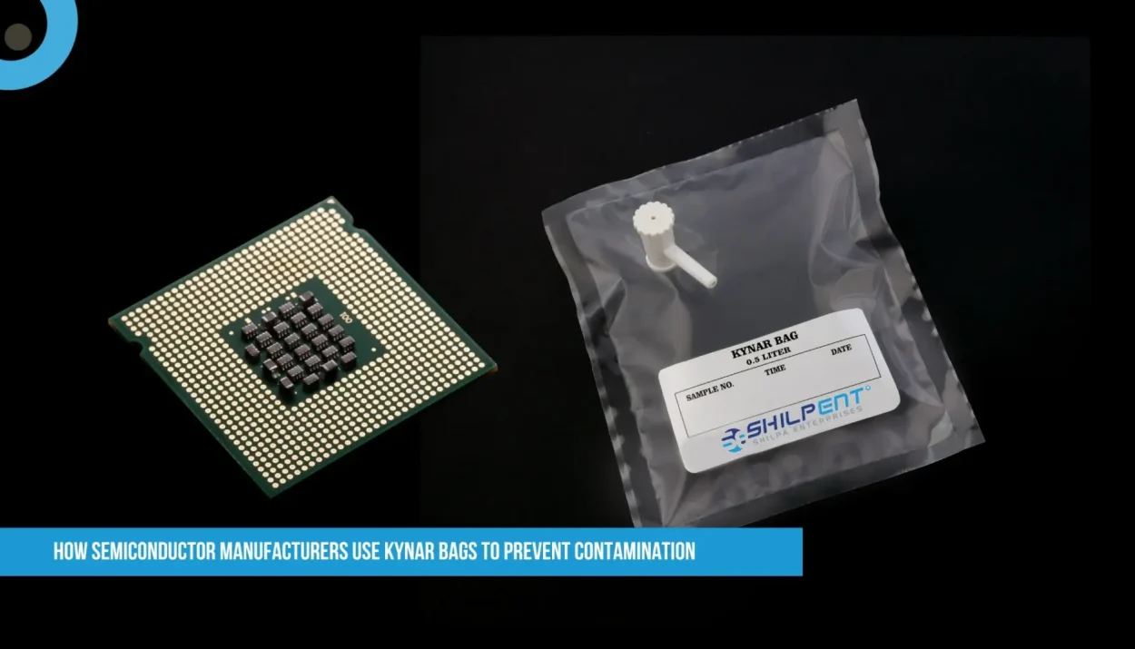
In the ultra-precision world of semiconductor manufacturing, even microscopic contaminants can ruin multi-million-dollar wafer batches. Traditional plastic bags often fail to meet the strict purity standards required in cleanrooms. This is where KYNAR® (PVDF) bags shine—offering low particulate shedding, chemical inertness, and electrostatic discharge (ESD) safety**. This article explores how leading chipmakers like Intel, TSMC, and Samsung rely on KYNAR bags to protect sensitive components.
Why Semiconductor Fabs Demand KYNAR Bags
Ultra-Low Particle Contamination
Problem: Standard polyethylene bags shed >500 particles/ft³ (per IEST-STD-CC1246D).
Kynar Bag Solution: PVDF’s smooth surface releases <10 particles/ft³, critical for Class 1-10 cleanrooms.
Case Study: A TSMC audit found 30% fewer defects after switching to KYNAR wafer bags.
Chemical Purity for Photolithography
Risk: Photoresist chemicals can degrade PVC or LDPE bags, leaching plasticizers.
Kynar Bag Advantage: Resists acetone, isopropanol (IPA), and TMAH —key solvents in chip production.
Data Point: – Applied Materials specifies KYNAR for EUV lithography mask storage.
ESD-Safe Protection
Static Hazard: Traditional plastics generate >1,000V static charges, risking CMOS damage.
KYNAR’s Edge: PVDF is inherently dissipative (10⁶–10⁹ Ω/sq), preventing electrostatic discharge.
Example: Intel’s 14nm FinFET process mandates ESD-safe KYNAR packaging.
Moisture Barrier for Hygroscopic Wafers
Challenge: Silicon wafers absorb moisture, causing oxidation and doping irregularities
KYNAR Performance:0.01 g/m²/day water vapor transmission rate (WVTR) vs. 0.5+ for HDPE.
Key Applications in Semiconductor Manufacturing
Wafer Transport & Storage
Process: 300mm wafers are sealed in double-layered KYNAR bags with nitrogen purging.
Industry Standard: SEMI S2/S8 compliant for front-opening unified pods (FOUPs).
Photomask Protection
Critical Need: A single EUV photomask costs $500K+ and is hypersensitive to particles.
Solution: KYNAR bags with anti-reflective coatings prevent haze formation.
Chemical Delivery Systems
Use Case: High-purity CMP slurries and etchants stored in KYNAR-lined containers.
Prevents: Metal ion leaching (e.g., Na⁺, K⁺) that alters doping profiles.
Equipment Component Packaging
Example: ASML’s EUV optics modules shipped in custom KYNAR pouches.
Challenges & Innovations
Cost vs. Benefit Analysis
KYNAR Cost 3–5× more expensive than LDPE bags.
ROI Justification: A single avoided wafer scrap saves $50K+ at 3nm nodes.
Sustainability Pressures
Recycling Hurdle: PVDF requires specialized pyrolysis (pioneered by companies like Arkema).
Emerging Alternative: Bio-based fluoropolymers in R&D (e.g., Solvay’s HYFLON®).
Smart Packaging Integration
Future Trend: KYNAR bags with printed graphene sensors to monitor:
Oxygen ingress (<1 ppm)
Vibration during transport
Conclusion
For semiconductor giants, KYNAR bags aren’t just packaging—they’re a critical contamination control strategy. By combining ultra-low particulates, chemical inertness, and ESD protection, PVDF enables the 3-nm-and-beyond era of chipmaking. As fabs push into GAAFET and CFET technologies, expect KYNAR innovations like self-sealing and RFID-trackable versions to become industry staples.
Key Takeaways
- Eliminates particle contamination in Class 1 cleanrooms
- Protects wafers from moisture, static, and chemical leaching
- Used by all top 10 semiconductor fabs (per SEMI reports)
- Higher cost justified by yield savings
- Future: Self-monitoring and sustainable PVDF solutions