When you look at a smartphone, computer, or even a solar panel, you’re looking at a modern marvel powered by one of the most essential materials in technology, the silicon wafer. These thin, flat discs of pure silicon may look simply, but they form the foundation of nearly all electronic devices we use today.
What is a Silicon Wafer?
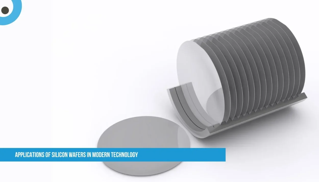
A silicon wafer is a skinny slice of crystalline silicon, usually circular, used as a base material for manufacturing electronic circuits and devices. Silicon is a semiconductor, meaning it can conduct electricity under certain conditions—making it ideal for controlling electrical signals in devices.
Key Applications of Silicon Wafers
Semiconductors and Microchips
This is the most common and critical application. Silicon wafers are used to create integrated circuits (ICs), the brains behind computers, smartphones, and almost every electronic gadget.
What they do: Microchips made from silicon wafers process data, store memory, and control everything from apps to cameras.
Where you see it: Laptops, smartphones, gaming consoles, tablets.
Solar Cells (Photovoltaics)
Silicon wafers are used to make solar panels that convert sunlight into electricity.
How it works: When sunlight hits a doped silicon wafer, it generates an electric current.
Where you see it: Rooftop solar panels, solar farms, solar-powered calculators.
Automotive Electronics
Modern cars are packed with electronic systems, many of which rely on silicon wafers.
Applications include Sensors, automatic braking systems, GPS, and battery management systems (especially in electric vehicles, or EVs).
Why it’s essential: Enhances safety, navigation, and performance.
Medical Devices
Silicon wafers are used in biosensors and diagnostic tools, allowing healthcare professionals to monitor and treat patients more effectively.
Applications include: Glucose sensors, heart monitors, and lab-on-a-chip devices.
Key Benefit: Offers accurate, real-time health monitoring.
Telecommunications
Silicon wafers are crucial for manufacturing components that process data and signals in telecommunication devices.
Applications include: Mobile networks (4G, 5G), satellite communications, and internet routers.
Result: Faster, more reliable internet and mobile connections.
MEMS (Micro-Electro-Mechanical Systems)
MEMS are tiny machines or sensors built on silicon wafers.
Where it’s used: Airbag sensors in cars, pressure sensors, microphones in smartphones, and inkjet printer heads.
Benefit: Enables tiny yet powerful systems.
Temperature and Pressure Sensors
These sensors are often created on silicon wafers for high accuracy and durability.
Used in: Industrial automation, HVAC systems, aerospace instruments.
Advantage: Withstands harsh environments and offers precise readings.
Cameras and Imaging Sensors
Silicon wafers are used to create CMOS and CCD sensors, which convert light into electrical signals for digital imaging.
Used in: Digital cameras, smartphone cameras, security systems.
Impact: Enables high-quality, compact imaging technology.
Consumer Electronics
From smartwatches to smart TVs, silicon wafers power many of the features in household electronics.
Function: Controls processors, memory, and touch interfaces.
Examples Include Smart speakers, e-book readers, and VR headsets.
Research and Development
Silicon wafers are widely used in laboratories and universities for testing new technologies.
Purpose: Used in prototyping, sensor development, and nanotechnology experiments.
Benefit: Helps bring innovations from lab to market.
Final Thoughts
Silicon wafers are more than just slices of material—they are the backbone of modern life. From the chips in our phones to the panels on our roofs, these tiny discs play a considerable role. As technology advances, particularly in fields such as AI, IoT, and renewable energy, the demand for high-quality silicon wafers is expected to continue growing.