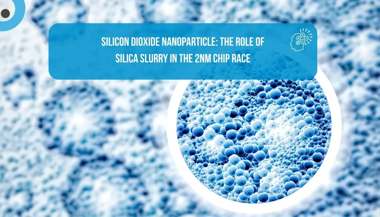
In the high-stakes race for the 2nm (2-nanometer) chip node, the spotlight often falls on massive photolithography machines. However, there is a quieter, microscopic hero essential to this revolution: Silica Slurry.
As transistors shrink to the size of a few dozen atoms, the surfaces they sit on must be perfectly flat. This is where Silicon Dioxide (SiO2) Nanoparticles come into play.
The Precision Problem: Why 2nm Needs Atomic Flatness
In semiconductor manufacturing, each layer of a chip must be perfectly flat before the next one is added. If a surface has even a microscopic hill or valley, the light used to etch the circuit will blur, much like a camera failing to focus on a wrinkled piece of paper.
At the 2nm level, the margin for error is nearly zero. Engineers use a process called Chemical Mechanical Polishing (CMP) to achieve this.
The Secret Sauce: Silicon Dioxide Nanoparticles
A CMP slurry is a liquid mixture containing chemically active agents and abrasive nanoparticles. Colloidal Silicon Dioxide Nanoparticle (SiO2) is the industry’s preferred abrasive for several reasons:
Nano-Scale Precision: The silica nanoparticles in these slurries are typically between 10nm and 100nm in size. Their spherical shape allows them to “roll” and “slide” across the wafer, gently buffing away irregularities without causing deep scratches.
Chemical Synergy: The slurry doesn’t just grind; it reacts. The chemicals soften the wafer’s top layer, and the SiO2 particles then wipe away the softened material.
Purity: For 2nm chips, even a single atom of a dirty metal can ruin a batch of 1,000 chips. Synthetic silica nanoparticles are produced with extreme purity to prevent contamination.
The 2nm Challenge: Selective Removal.
In 2nm architectures (such as GAAFETs or Nanosheets), different materials, such as Silicon, Germanium, and Silicon Nitride, are packed tightly together.
The slurry must be smart enough to polish the Silicon Dioxide layers while stopping the moment it hits a Silicon Nitride stop-layer. Modern silica slurries are engineered for High Selectivity, meaning they can be tuned to remove one material 5 to 10 times faster than another, ensuring the delicate 2nm structures remain intact.
Conclusion: The Future is Polished
The 2nm chip race isn’t just about who has the best lasers; it’s about who has the best chemistry. Without the extreme precision of Silicon Dioxide Nanoparticles in modern slurries, the layers of tomorrow’s AI processors would simply be too rough to function.
As we look toward 1nm and beyond, the polish will become just as high-tech as the print.