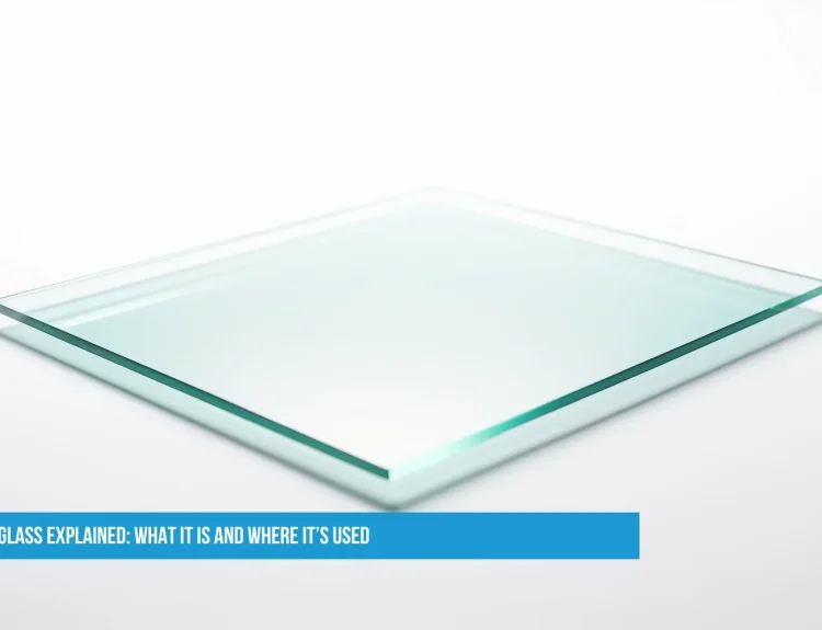
If you’ve ever looked at a silicon wafer, it looks like a shiny, metallic disc. But to a chipmaker, that wafer is a complex and precisely engineered foundation. Its specifications determine what kind of amazing chips can be built upon it—from the processor in your phone to the memory in your laptop.
The three most essential specs you’ll encounter: Dopants, Orientation, and Resistivity.
Dopants: The “Personality” of the Silicon
The Simple Idea: Pure silicon is a semiconductor; it’s okay at conducting electricity, but not great. To make it worthwhile for transistors (the tiny on/off switches in chips), we need to control their conductivity. We do this by adding small, intentional impurities called dopants. This process is called doping.
Think of it like this: Pure silicon is a neutral party. Adding a dopant gives it either a negative or positive personality.
N-Type (Negative) Silicon:
Dopant Used: Elements like Phosphorus or Arsenic. These have one extra electron in their outer shell compared to silicon.
The Result: This extra electron is free to move around, carrying a negative charge. Silicon doped this way is called N-Type because its primary charge carriers are negative electrons.
P-Type (Positive) Silicon:
Dopant Used: Elements like Boron. This has one fewer electron in its outer shell compared to silicon.
The Result: This creates a “hole” (a spot where an electron is missing), which acts like a positive charge carrier. Silicon doped this way is called P-Type because its primary charge carriers are positive holes.
Why it matters: By creating regions of P-Type and N-Type silicon right next to each other on a wafer, engineers build the fundamental building block of all modern electronics: the PN junction, which is the heart of diodes and transistors.
Buy Silicon Wafer from trusted brands
Crystal Orientation: The “Atomic Blueprint”
The Simple Idea: A silicon wafer isn’t a random jumble of atoms. It’s a perfect single crystal, meaning its atoms are arranged in a continuous, repeating 3D pattern called a lattice (like a perfectly stacked grid of eggs).
However, this grid can be sliced in different directions. These different slices are referred to as crystal orientations.
The orientation is described by numbers in parentheses, such as (100), (111), or (110). These “Miller indices” are a mathematical method for describing the angle of the slice.
Why it matters:
(100) Wafers: This is the most common type. They have the best surface quality for growing a layer of silicon dioxide (the crucial insulator in transistors) and are the standard for most computer chips (CMOS technology).
(111) Wafers: These have a different atomic structure at the surface. They are often used for other purposes, such as making MEMS devices or as substrates for growing other materials. Their properties are better suited for these specific jobs.
Think of it like cutting wood: you can cut with the grain, against the grain, or at an angle. Each cut results in a surface with different properties. Chip designers choose the wafer orientation that gives them the best “surface” to build on.
Resistivity: The “Traffic Report”
The Simple Idea: Resistivity is a measure of how strongly the silicon material “resists” the flow of electrical current. It’s the inverse of conductivity.
Low Resistivity: Means it’s easier for current to flow. The material is a better conductor.
High Resistivity: Means it’s harder for current to flow. The material is a better insulator.
What controls resistivity? The amount of dopant added.
Adding more dopant creates more free electrons or holes, making it easier for current to flow. This results in LOW resistivity.
Adding less dopant creates fewer charge carriers, making it harder for current to flow. This results in HIGH resistivity.
Why it matters: Resistivity is critical for performance.
Transistor Channels: The area under a transistor’s gate needs precisely controlled resistivity to turn on and off correctly.
Power Loss: In high-power applications, low-resistivity wafers are needed to minimize energy loss as heat.
Signal Integrity: In high-frequency applications (like 5G phones), specific resistivity is needed to ensure signals are clean and don’t degrade.
Think of it like a highway:
Low Resistivity = A broad, open highway with no traffic (current flows easily).
High Resistivity = A narrow, congested road with many stop signs (the current has a hard time getting through).
How It All Works Together
When an engineer orders wafers to produce a specific chip, they don’t simply request “silicon wafers.” They specify a precise recipe:
> “I need a <u>P-Type</u>, <u>(100) </u> orientation wafer with a <u>resistivity</u> of 1-10 Ohm-cm.”
This tells the wafer manufacturer exactly how to engineer the foundation so that the billions of transistors built on top of it will perform as expected. By controlling the dopant (personality), orientation (blueprint), and resistivity (traffic flow), we can create the incredible variety of chips that power our world.


