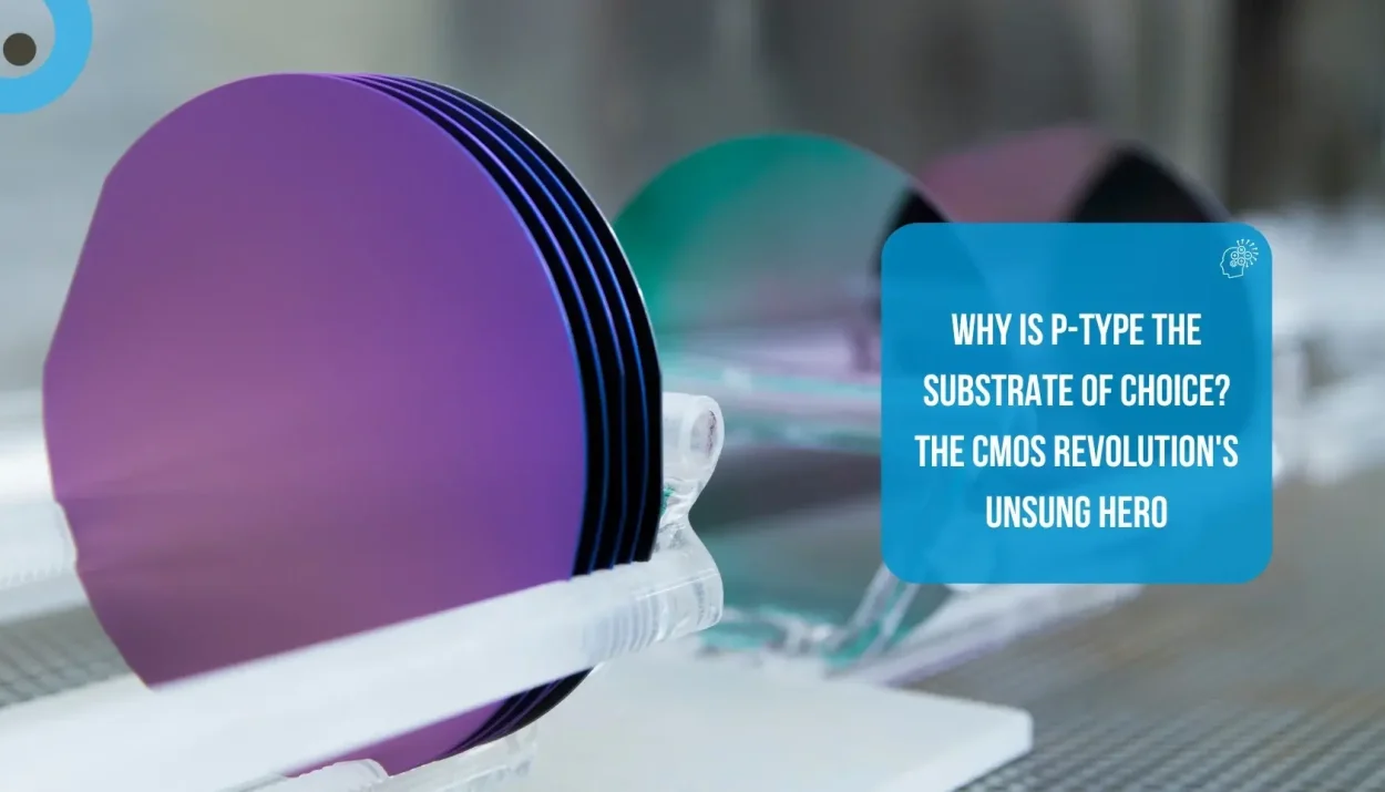
If you examined the microchip inside your phone or laptop, you would see a silicon wafer forming the base for billions of microscopic switches. For decades, the industry has consistently selected one specific type of silicon for this base: P-Type.
In a world obsessed with the latest processor speeds, the humble substrate is often overlooked. But without P-type silicon, the digital revolution might have been slower, hotter, and more expensive. Here is why this specific material became the unsung hero of the CMOS revolution.
The Need for Speed (Electrons vs. Holes)
To understand the substrate, we have to look at the physics of electricity. In silicon, current is carried by two things:
- Electrons: Negatively charged particles.
- Holes: The “empty seats” where electrons used to be (positively charged).
A key point is that electrons in silicon have a mobility approximately 2 to 3 times higher than that of holes.
Because electrons are the “sports cars” of the atomic world, engineers prioritize transistors that use them (NMOS transistors). To build a great NMOS transistor, you need a P-Type foundation. It is simply the best soil for growing the fastest crops.
Buy Silicon Wafers:
The N-Well Standard
Modern chips use CMOS (Complementary Metal-Oxide-Semiconductor) technology, which combines NMOS and PMOS transistors. These transistors require electrical isolation to function properly.
Since NMOS transistors, with higher performance, are preferred, they are fabricated directly in the P-type substrate. PMOS transistors are formed within isolated N-wells embedded in the P-type substrate.
By making the P-type substrate the standard, manufacturers prioritized the performance of the faster, more efficient NMOS devices.
Cosmic Protection and Purity
Surprisingly, P-type silicon inherently resists contamination more effectively.
During the intense heat of manufacturing, impurities such as iron or copper can sneak into the silicon lattice, ruining chips. P-type silicon (doped with Boron) has a unique ability to trap these impurities away from the active transistors. It acts like a built-in trash collector, leading to higher yields and fewer broken chips.
Resistance to Radiation
For chips used in space or high-altitude flights, radiation is a killer. It turns out that P-type silicon is generally more radiation-resistant than N-type silicon.
While N-type solar cells are gaining traction recently for efficiency, the logic chips (CPUs/GPUs) that run the world remain firmly rooted in P-type due to historical reliability and robustness.
Conclusion
The choice of P-type silicon wasn’t an accident; it was a calculated decision to prioritize speed and reliability.
By choosing a foundation that favors the fast-moving electron, engineers created an infrastructure akin to a well-designed highway, allowing computing speeds to double year after year. P-type silicon may look like a simple slice of grey crystal, but, like a blank canvas for an artist, it serves as the essential base upon which the modern world is built.