
Silicon wafers are among the most important materials in modern science and technology. Serving as the foundation for semiconductor devices, these ultra-flat and highly pure silicon substrates are used in the fabrication of integrated circuits, sensors, photovoltaic cells, microelectromechanical systems (MEMS), and advanced research devices.
From smartphones and computers to solar panels and laboratory instruments, countless technologies rely on silicon wafers as the platform upon which electronic functionality is built. Their exceptional material properties, combined with decades of manufacturing refinement, have made silicon the dominant semiconductor material worldwide.
What is a Silicon Wafer?
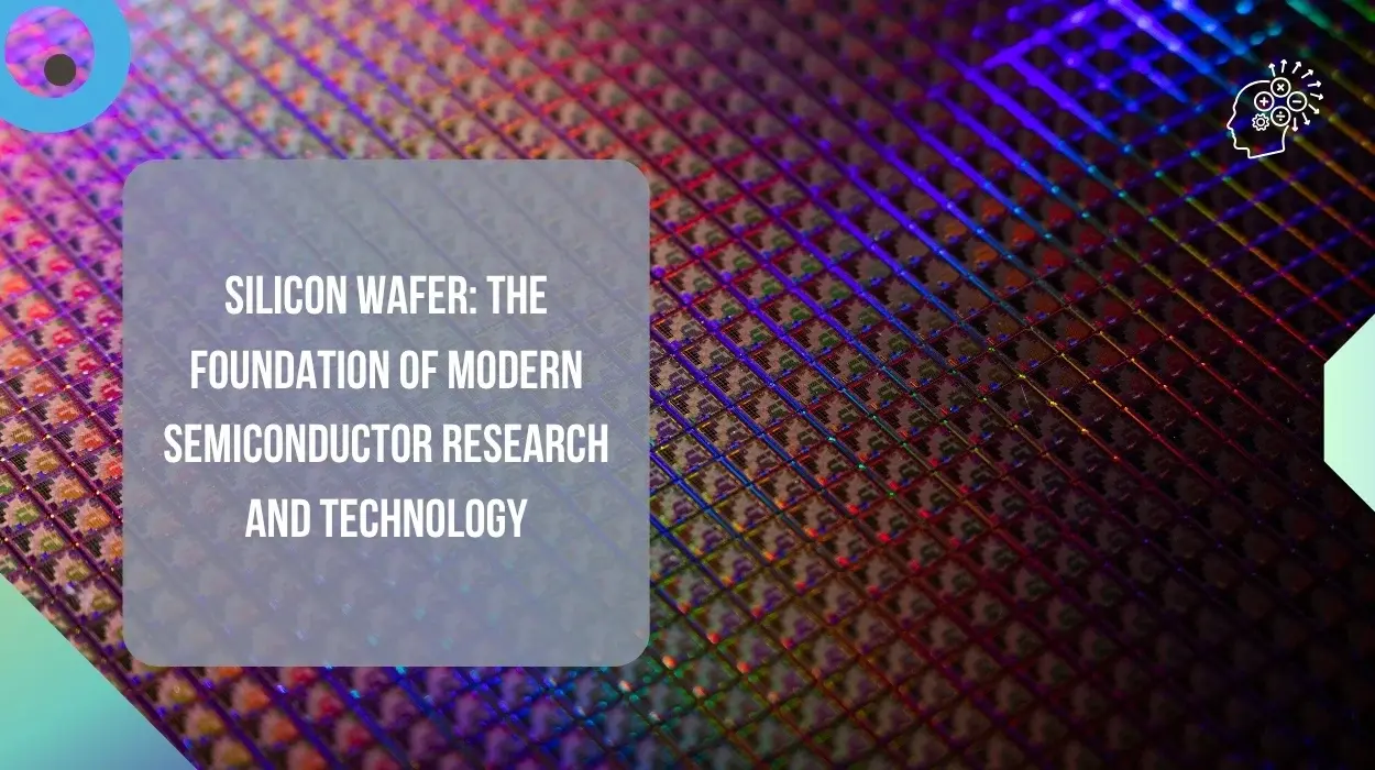
A silicon wafer is a thin, circular slice of highly purified crystalline silicon. It acts as a substrate on which electronic, optical, and microfabricated structures are created through a series of deposition, patterning, and etching processes.
The wafer serves as a stable and uniform platform for building complex semiconductor devices with microscopic precision. Depending on the intended application, silicon wafers may be supplied in various diameters, thicknesses, crystal orientations, and surface finishes.
Why Silicon is the Preferred Semiconductor Material
Silicon has become the material of choice for semiconductor manufacturing because it offers an ideal balance of electrical, thermal, mechanical, and economic advantages.
Excellent Semiconductor Properties
Silicon possesses electrical characteristics that allow precise control of electron flow, making it suitable for transistors, diodes, and integrated circuits.
High Material Purity
Modern manufacturing techniques enable silicon to be produced with extremely low impurity levels, ensuring reliable device performance.
Thermal Stability
Silicon maintains its structural integrity and electrical properties across a wide temperature range, making it suitable for demanding applications.
Abundant Availability
As one of the most abundant elements on Earth, silicon provides a cost-effective foundation for large-scale technological development.
Strong Mechanical Strength
Silicon wafers exhibit excellent dimensional stability and can withstand the complex processing steps involved in device fabrication.
Manufacturing of Silicon Wafers
The production of silicon wafers begins with the purification of silicon to achieve semiconductor-grade quality. A single-crystal silicon ingot is then grown using specialized crystal growth techniques.
The ingot is sliced into thin wafers, followed by precision grinding, polishing, and cleaning processes. The final product possesses an exceptionally smooth surface suitable for advanced microfabrication and nanotechnology applications.
The quality of a silicon wafer is determined by factors such as crystal structure, flatness, surface roughness, defect density, and dimensional accuracy.
Types of Silicon Wafers
Single Crystal Silicon Wafer
Single crystal wafers possess a continuous and uniform crystal structure throughout the substrate. They are widely used in semiconductor manufacturing and scientific research due to their superior electrical properties.
Double Side Polished Wafer
These wafers are polished on both sides to achieve high surface quality and dimensional precision, making them suitable for optical devices, MEMS, and advanced research applications.
Single Side Polished Wafer
Single side polished wafers have one mirror-finished surface and are commonly used in standard semiconductor and solar cell fabrication processes.
Undoped Silicon Wafer
Undoped wafers contain minimal intentional impurities and are frequently used in research and specialized electronic applications.
Doped Silicon Wafer
Doped wafers contain controlled amounts of impurities to modify electrical conductivity and support specific device requirements.
Key Characteristics of Silicon Wafers
Silicon wafers are valued for several important characteristics:
- High crystalline purity
- Excellent electrical properties
- Smooth and defect-free surface
- Superior thermal stability
- Precise dimensional control
- Compatibility with advanced fabrication techniques
- Long-term reliability
- Excellent mechanical strength
These properties make silicon wafers indispensable in both research laboratories and industrial manufacturing environments.
Applications in Scientific Research
Semiconductor Device Development
Researchers use silicon wafers to fabricate experimental transistors, diodes, integrated circuits, and microelectronic components.
Nanotechnology Research
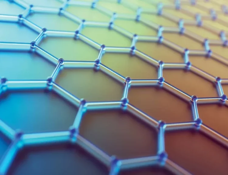
Silicon wafers serve as substrates for studying nanomaterials, thin films, nanoparticles, graphene, and nanoscale device architectures.
MEMS Fabrication
Microelectromechanical systems such as pressure sensors, accelerometers, microfluidic devices, and actuators are commonly fabricated on silicon wafers.
Photovoltaic Research
Scientists utilize silicon wafers in solar energy research to investigate improved photovoltaic materials, device structures, and energy conversion efficiencies.
Sensor Development
Silicon-based sensors are widely researched for applications in environmental monitoring, healthcare diagnostics, industrial automation, and smart devices.
Thin Film Deposition Studies
Researchers frequently deposit metals, oxides, semiconductors, and functional coatings onto silicon wafers to evaluate material performance and device behavior.
Silicon Wafers in the Electronics Industry
The global electronics industry is built upon silicon wafer technology. Modern microprocessors, memory devices, communication chips, and power electronics all begin with a silicon substrate.
Advancements in wafer processing have enabled the creation of increasingly powerful and compact electronic devices while reducing manufacturing costs and improving efficiency.
As demand for artificial intelligence, high-performance computing, and connected devices grows, silicon wafers continue to play a central role in technological progress.
Importance in Renewable Energy
Silicon wafers are the primary material used in crystalline silicon solar cells, which account for a significant portion of global solar energy production.
Their ability to efficiently convert sunlight into electricity has contributed to the widespread adoption of solar power as a sustainable energy source. Ongoing research aims further to improve efficiency, durability, and manufacturing techniques.
Future Trends and Innovations
Emerging technologies are expanding the capabilities of silicon wafer-based systems. Research efforts are focused on advanced semiconductor architectures, quantum devices, integrated photonics, flexible electronics, and next-generation sensors.
The combination of silicon with novel materials such as graphene, transition metal compounds, and nanostructured coatings is creating new opportunities for scientific discovery and industrial innovation.
Conclusion
Silicon wafers form the technological backbone of modern electronics, renewable energy systems, and scientific research. Their exceptional purity, stability, and semiconductor properties make them indispensable for the fabrication of advanced devices and experimental technologies.
From microchips and sensors to solar cells and nanotechnology, silicon wafers continue to enable breakthroughs that shape the future of science, engineering, and global technological development. As research and manufacturing techniques evolve, silicon wafers will remain a fundamental platform for innovation across countless industries and applications.