
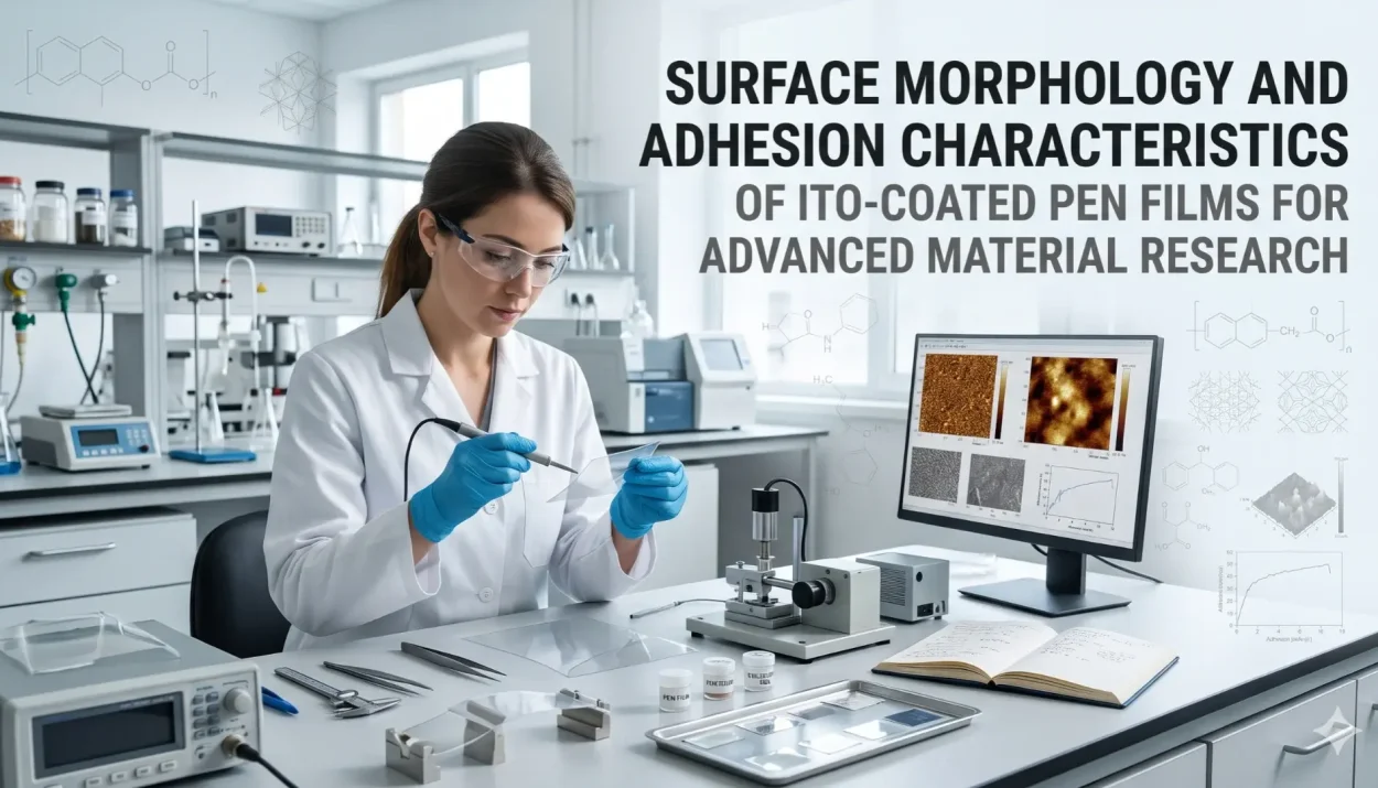
Indium Tin Oxide (ITO) coated Polyethene Naphthalate (PEN) films have gained considerable attention in advanced material research due to their combination of optical transparency, electrical conductivity, thermal stability, and mechanical flexibility. These films consist of a thin ITO conductive layer deposited on a PEN polymer substrate, creating a functional material suitable for applications requiring transparent, electrically conductive surfaces.
The performance of ITO-coated PEN films depends not only on their electrical and optical properties but also on the surface morphology and adhesion characteristics of the deposited coating. Surface uniformity, grain distribution, coating continuity, and interfacial bonding significantly influence the reliability and functional stability of these materials.
Understanding these characteristics is essential for developing high-performance transparent conductive films for flexible electronics, optoelectronic devices, thin-film research, and advanced material engineering.
Understanding the Surface Morphology of ITO-Coated PEN Films
Surface morphology describes the physical structure and surface characteristics of a material at microscopic and nanoscale levels. In ITO-coated PEN films, it refers to the distribution, texture, uniformity, and continuity of the ITO layer deposited over the polymer substrate. A well-developed ITO coating generally exhibits a relatively uniform surface with consistent grain distribution and minimal visible defects.
These characteristics contribute to predictable electrical behaviour and improved functional performance. Several surface features are particularly important:
Surface Uniformity: A consistent coating distribution helps maintain uniform electrical characteristics across the film. Variations in coating thickness or surface coverage can create localised differences in conductivity.
Grain Structure: The size, shape, and arrangement of ITO grains influence the microstructure of the conductive layer. Grain boundaries and their distribution can affect electron transport and overall film performance.
Surface Roughness: Surface roughness plays an important role in determining the contact characteristics and suitability of ITO-coated PEN films for subsequent thin-film deposition processes.
Coating Continuity: A continuous conductive layer supports consistent electrical pathways. Pinholes, cracks, and discontinuities may affect the film’s electrical response and reliability.
Adhesion Characteristics Between ITO and PEN Layers
Adhesion is a critical property that determines how effectively the ITO coating remains attached to the PEN substrate during handling, processing, and practical use. The ITO-PEN interface involves interactions influenced by surface energy, substrate preparation, deposition conditions, and the physical characteristics of the deposited coating.
Strong interfacial adhesion is desirable because it helps prevent coating separation, peeling, and defect formation during mechanical handling. Important factors influencing adhesion include:
Substrate Surface Preparation: Cleaning and appropriate surface treatment can remove contaminants and improve the surface condition before ITO deposition.
Deposition Conditions: Parameters such as deposition temperature, sputtering power, working pressure, and deposition rate can influence film growth and interfacial characteristics.
Surface Energy: The surface properties of PEN can affect how effectively the deposited ITO layer contacts the polymer substrate.
Coating Thickness: ITO layer thickness can influence internal stress and mechanical behaviour. Excessive coating thickness may increase the possibility of cracking or interfacial failure under certain conditions.
Thermal Compatibility: Differences in thermal expansion and dimensional behaviour between ITO and PEN may generate interfacial stress during temperature variations.
Microstructural Analysis and Surface Characterisation
Scientific characterisation techniques provide valuable information about the structural quality and interfacial properties of ITO-coated PEN films. Several analytical methods can be used to investigate their surface morphology and adhesion characteristics.
Scanning Electron Microscopy (SEM)
Scanning Electron Microscopy is widely used to examine surface features at high magnification. It helps researchers identify grain distribution, surface defects, coating discontinuities, microcracks, and structural variations. SEM analysis can also provide useful information about the uniformity of the deposited conductive layer.
Atomic Force Microscopy (AFM)
Atomic Force Microscopy enables nanoscale examination of surface topography. It provides information about surface roughness, local height variations, and morphological features. AFM characterisation is particularly useful for understanding how surface texture changes with different deposition conditions.
Optical Microscopy
Optical microscopy offers an initial assessment of coating uniformity and visible surface defects. It can help identify scratches, contamination, localised damage, and larger structural irregularities.
Adhesion Testing
Adhesion testing evaluates the bonding strength between the ITO coating and PEN substrate. Depending on the film construction and research requirements, suitable methods may include cross-cut testing, tape testing, scratch testing, and controlled mechanical bending evaluations. These tests help determine whether the conductive layer maintains its adhesion under different handling and mechanical conditions.
Influence of Surface Morphology on Electrical Performance
The surface structure of ITO-coated PEN films has a direct relationship with their electrical behaviour. A relatively uniform and continuous ITO layer supports consistent conductive pathways across the substrate. However, structural imperfections such as cracks, pinholes, and uneven coating regions may interrupt these pathways. Grain boundaries can also influence charge transport within the conductive layer.
Their distribution, together with film density and microstructural quality, contributes to the overall electrical characteristics. For research applications, sheet resistance measurements using a four-point probe system can help evaluate electrical uniformity across different regions of the film. Combining electrical measurements with SEM and AFM observations provides a more comprehensive understanding of the relationship between surface morphology and conductive performance.
Mechanical Stability and Interfacial Reliability
ITO-coated PEN films are particularly interesting for research involving flexible conductive substrates. Their mechanical behaviour depends on the interaction between the relatively brittle ITO coating and the flexible PEN polymer base. During bending or repeated deformation, mechanical stress can develop within the conductive layer and at the interface between the two materials.
Depending on coating thickness, deposition conditions, bending radius, and substrate characteristics, this stress may lead to microcrack formation, changes in electrical resistance, or partial coating separation. Repeated bending studies can therefore provide useful information about the mechanical reliability of these films.
Researchers can evaluate changes in surface morphology before and after bending cycles using microscopy techniques, while electrical measurements can help identify changes in conductive performance.
Research Applications of ITO-Coated PEN Films
The combination of transparency, conductivity, and polymer flexibility makes ITO-coated PEN films useful in several advanced material research areas.
Flexible Electronics: These films can serve as transparent conductive substrates in experimental flexible electronic structures.
Optoelectronic Research: Their optical and electrical characteristics make them suitable for investigating transparent electrodes and light-responsive device architectures.
Thin-Film Deposition Studies: ITO-coated PEN substrates provide a platform for studying the growth, adhesion, and structural behaviour of additional functional thin-film layers.
Flexible Sensors: Their conductive surface and flexible substrate structure offer opportunities for developing experimental sensing platforms.
Photovoltaic Research: Transparent conductive ITO layers can be investigated as electrode components in flexible photovoltaic structures.
Challenges and Future Research Opportunities
Despite their promising properties, ITO-coated PEN films present several research challenges. Maintaining consistent coating adhesion while preserving flexibility remains an important material engineering consideration. Researchers must also investigate how deposition conditions affect grain structure, surface roughness, residual stress, and electrical uniformity.
Future research can focus on developing improved substrate surface treatments, optimising thin-film deposition parameters, and understanding the relationship between microstructural characteristics and long-term coating stability. Another important research direction is examining how environmental exposure, temperature variations, and repeated mechanical deformation influence the ITO-PEN interface.
Combining surface characterisation, adhesion evaluation, and electrical measurements can help establish a more comprehensive understanding of these materials.
Conclusion
ITO-coated PEN films represent an important class of transparent conductive polymer substrates for advanced material research. Their performance is strongly influenced by the surface morphology of the ITO layer and the quality of adhesion between the conductive coating and PEN substrate.
Surface uniformity, grain distribution, coating continuity, interfacial bonding, and mechanical stability are essential characteristics that determine the functional reliability of these films. Advanced characterisation techniques such as SEM, AFM, optical microscopy, and adhesion testing provide valuable insights into their structural and interfacial behaviour.
As research into flexible and transparent materials continues to expand, ITO-coated PEN films offer considerable opportunities for investigating next-generation conductive substrates and advanced thin-film structures.